EDX-PCB
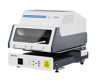
Top-illumination XRF coating-thickness analyzer with a very large travel range — for measuring large PCB boards, enclosures and wafers, with drawing and image input.
- Very large travel range for big samples
- Measurement of large PCB boards, enclosures and wafers
- Drawing-input system and external image import
- Micro-area camera for fast point positioning
- Fast programming and multi-point measurement
- Top-illumination XRF design
The EDX-PCB is a top-illumination X-ray coating-thickness analyzer with a very large travel range, designed for measuring large PCB boards, enclosures and wafers. It works with a drawing-input system and external image import, so you can freely and quickly move the sample to any area. A micro-area camera enables very fast positioning of even small measurement points, with efficient programming and execution of measurement series.
Applications
- Coating-thickness measurement on large PCB boards
- Inspection of large enclosures and assemblies
- Micro-area measurements on wafers
- Quality control in electronics
What to ask about
A large travel range and drawing input let you automate measurements on large, complex parts that standard thickness gauges cannot handle. Contact us to match a configuration to your boards and assemblies.
The full technical specification and configuration will be provided in the datasheet PDF.
Datasheet (PDF) — coming soon